In 2020, the global semiconductor supply chain looked like a triumph of efficiency. One foundry in Taiwan produced the most advanced logic chips on earth. A few equipment makers in the Netherlands and Japan built the machines that made those chips possible. The design software came from three American firms. The materials came from Japan and South Korea. The whole system ran on a just-in-time choreography that delivered the silicon underneath every phone, every data center, every car, every weapon system.
Then it broke. COVID closures exposed how little redundancy there was. The auto industry alone lost a forecasted $210 billion in revenue in 2021 because it could not get chips (AlixPartners, September 2021). And the geopolitics surfaced what had been left unsaid: the most strategic technology of the century was being manufactured 110 miles from a country the West treats as an adversary. The export shock that followed, first quiet, then formal, made one thing clear. The supply chain was never a market outcome. It was a policy outcome that nobody had bothered to defend. What came next was the largest coordinated industrial policy intervention in advanced economies since the Cold War. This matters to BITKRAFT, and not as background reading. The policy response redrew where physical compute gets built, funded, and scaled, and compute is the layer underneath almost everything we back. We already invest in the foundational infrastructure of AI-native experiences: video generation (Higgsfield), runtime for interactive agents (Inworld), GPU edge infrastructure (Radian Arc), brain-computer interfaces (OpenBCI), and a next-generation chip company still in stealth. So the question is narrow and practical. Where does this wave of policy actually create companies worth owning, and does our vantage point give us an edge in spotting them?
The scope of this piece is semiconductors and the hardware that lives in the same gravity well: chip architecture, photonics, advanced packaging, power electronics, the design toolchain, and the silicon being built specifically for AI inference. The capital dynamics and physics of biotech, fusion, or space are different problems and sit outside it. What ties this set together is that the same industrial policy, the same supply-chain bifurcation, and the same return of hardware as a fundable category are bending all of it at once.
The policy is unprecedented in scale
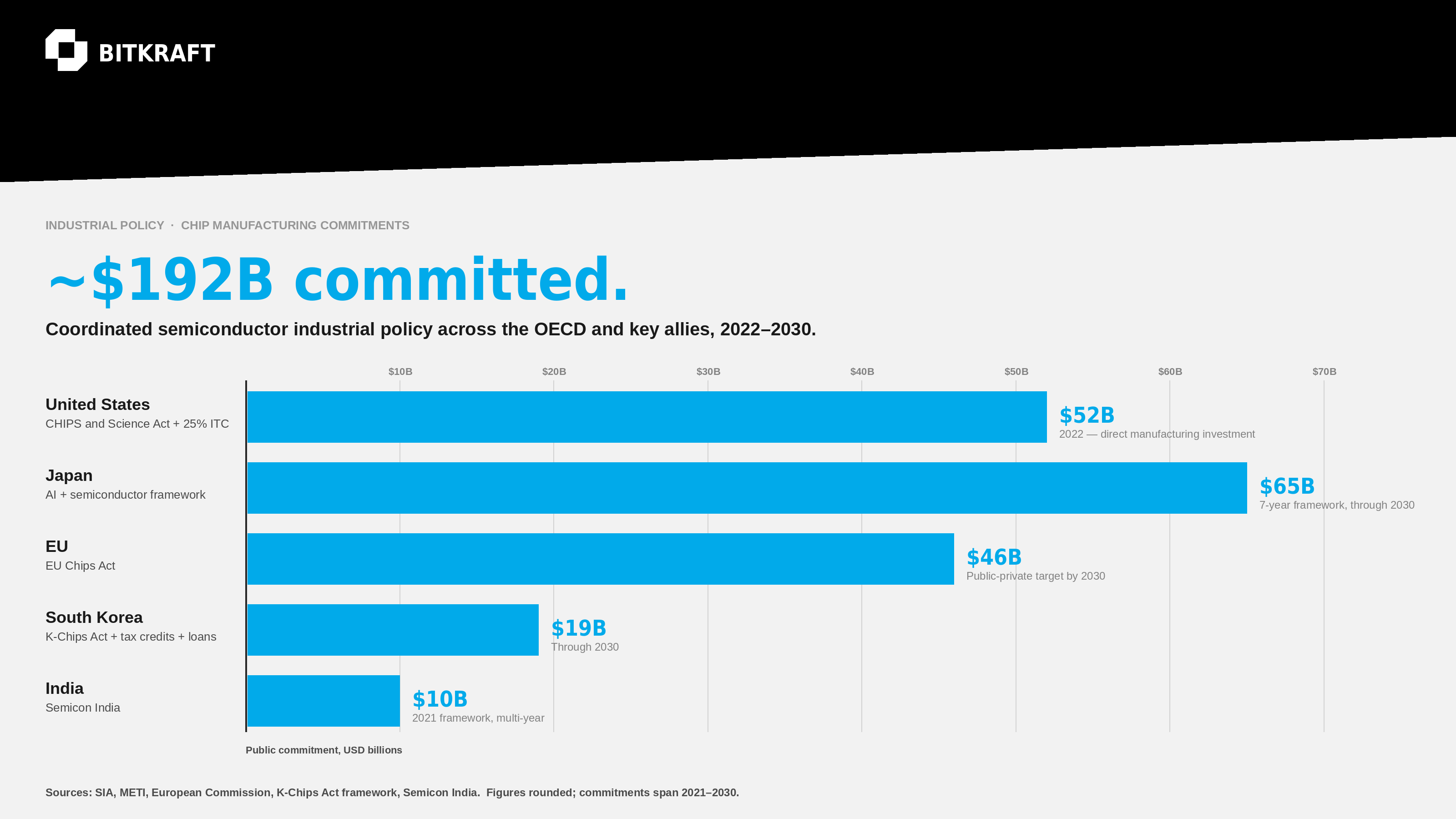
The CHIPS and Science Act, signed into US law in August 2022, put $52 billion behind domestic semiconductor manufacturing, plus a 25% investment tax credit on top. The EU Chips Act followed in 2023 with a €43 billion target. Japan committed multiple trillions of yen across successive packages and is funding a leading-edge foundry effort directly. South Korea answered with a support package of roughly ₩26 trillion, around $19 billion. India set aside $10 billion under its Semicon India program. Inside roughly eighteen months, the major OECD economies plus key allies had committed well north of $190 billion to rebuild chip capacity inside their own borders.
Governments have shaped technology markets before. DARPA seeded the internet. SEMATECH helped revive the US chip industry in the late 1980s. South Korea built memory dominance through coordinated state investment in the 1990s. Two things make this moment different. The scale, in real terms, is larger than anything since Apollo. And the coordination across countries is new. The CHIPS Act and the EU Chips Act were not drafted in isolation. They were written with awareness of each other and of the export-control regime being built alongside them. The G7 Hiroshima communiqué in 2023 made that coordination explicit. The May 2023 communiqué named semiconductors, critical minerals, and batteries as supply chains of collective concern and reaffirmed coordinated export controls on dual-use technology.
The export-control side matters as much as the subsidies. Starting October 7, 2022 and tightening through 2023 and 2024, the US Bureau of Industry and Security restricted advanced compute exports to China. Nvidia A100 and H100 shipments were curtailed, with the cutoff line drawn deliberately at the A100’s performance. The entity list grew. Allies followed on the equipment side: the Netherlands restricted DUV lithography in 2023, and Japan added controls on 23 categories of chipmaking gear that July. The cumulative effect is a bifurcated supply chain. There is now a Western stack and a Chinese stack, with a contested middle that runs through much of Southeast Asia and the Gulf.
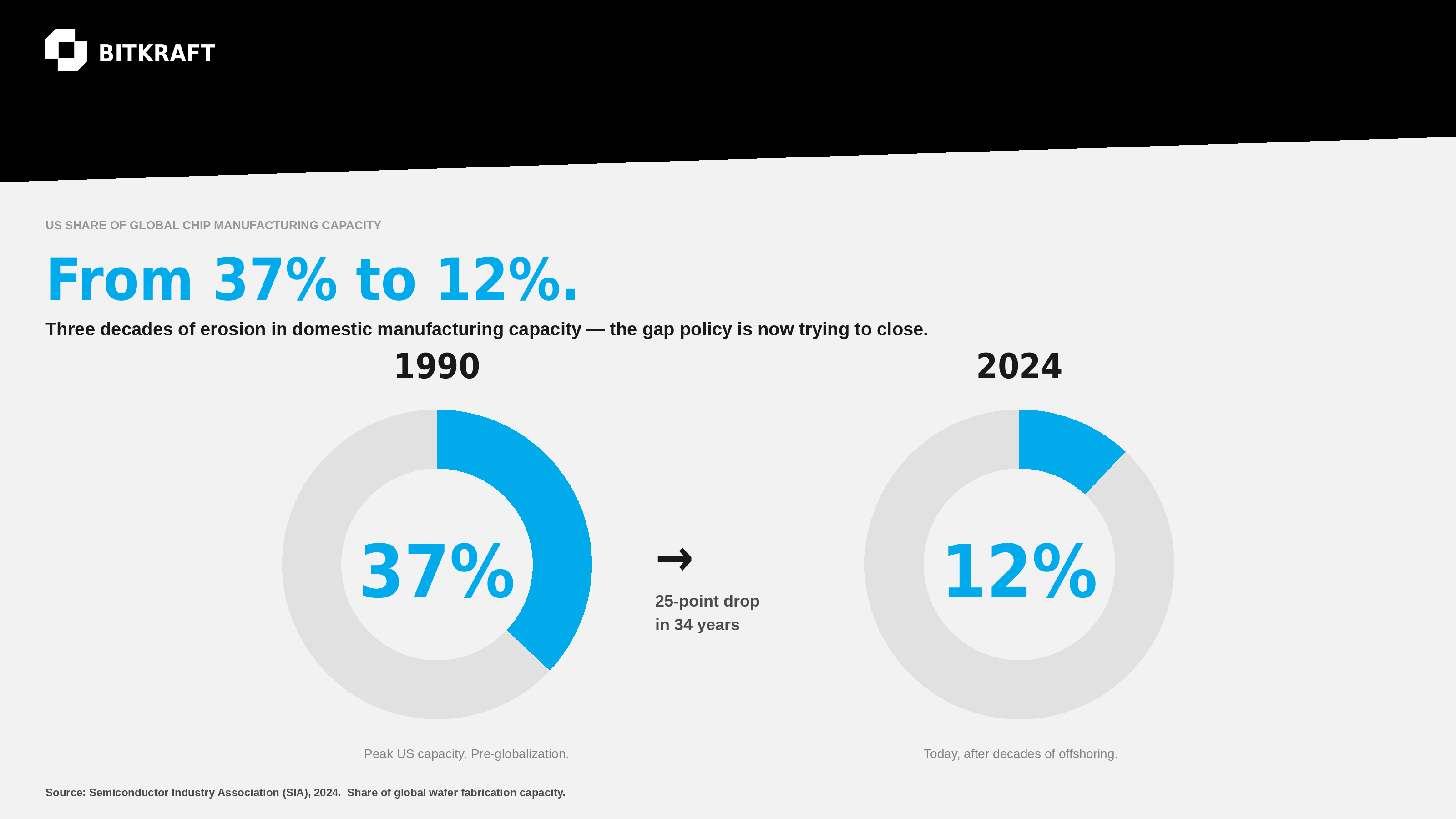
Two facts should anchor how investors read this. The US share of global chip manufacturing capacity sits at roughly 12% today, down from 37% in 1990 (SIA). And closing even part of that gap will take a decade of sustained capital that the private market alone would never underwrite. Policy here is not a tailwind. It is the wind.
What policy actually does, and what it does not
It is tempting to read all of this as a story about policy producing innovation. It does not, and it is worth being precise, because the sloppy version of this argument leads to bad investing. Industrial policy does not create breakthroughs. Breakthroughs come from people: physicists, materials scientists, and engineers solving problems that were hard long before any subsidy existed. What policy does is move money and attention. It makes some problems fundable that were not fundable before, protects some incumbents, and exposes others. The causation runs through talent and capital availability, not through the policy itself.
That distinction matters because of where the money has actually landed. Look at what the CHIPS Act pays for. The bulk of direct investment supports leading-edge logic and memory at the most advanced nodes. Intel, TSMC, Samsung, Micron, and a few others have committed to fabs in Arizona, Ohio, Texas, and New York. These are necessary. They are also iterative. They extend the existing CMOS roadmap and relocate it onto domestic soil. They do not change the underlying architecture of computing. The same has played out globally. Subsidies have mostly pulled incumbents’ fabs across borders. The new architecture work is happening in segments the policy money barely touches.
Why does the frontier sit outside the subsidy flow? Because of who can move and who cannot. A leading-edge logic fab costs $20 billion or more and runs only the architectures it was built for. The incumbents taking CHIPS Act money are economically locked into the roadmap they already have. They are the least likely actors to introduce a fundamentally different way to compute. That work happens in university spinouts and small teams of physics-first founders, on problems considered uninvestable five years ago. What changed is not the science. It is that capital following the policy created a runway long enough for these companies to survive the years between a working device and a manufacturable product.
This is the seam. Policy intent is to rebuild domestic capacity in advanced chips. Incumbent delivery is an iterative extension of the existing roadmap, now onshored. The gap between the two is where founders with new architectures and new materials get to do work that would not otherwise be funded. These companies are not usually taking CHIPS Act money directly. They benefit from the ecosystem the policy built: a denser pool of materials scientists, a more credible domestic supply chain for specialized processes, and a wave of attention that made hardware a fundable category again after a decade in the wilderness.
The seam has a second problem, and it is the more interesting one
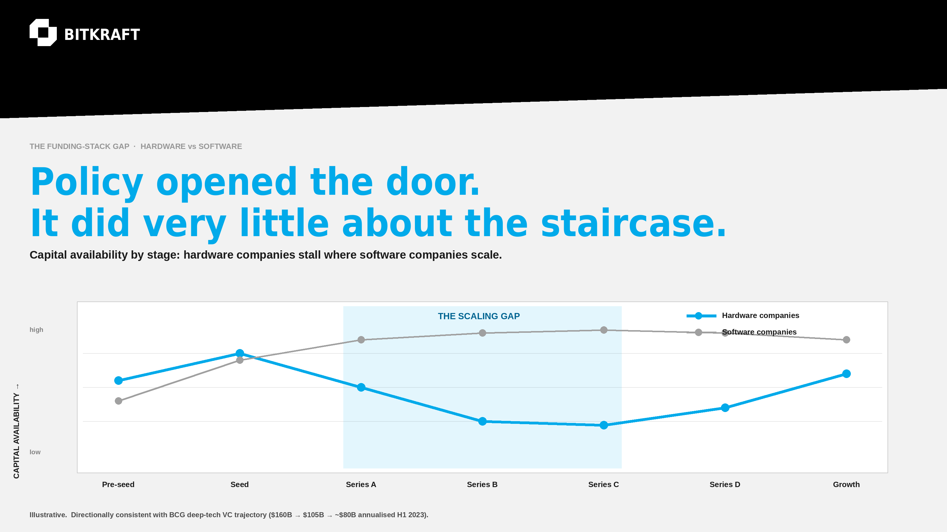
There is a flaw in the funding stack that does not get discussed enough, and it is the part of this thesis that matters most. Policy and a falling cost-to-prototype have made it easier than ever to start a hardware company. The bench of early-stage managers who can write the first checks into physics-first founders is deep and getting deeper. The problem is what comes next. The funds that write the Series A, B, C, and D, the rounds that carry a semiconductor company from a working device through manufacturing scale-up, are largely missing. And those rounds are bigger and more capital-intensive than their software equivalents. The direction of travel shows up in the aggregate data: BCG estimates deep-tech VC fell from roughly $160B in 2021 to about $105B in 2022 and roughly $80B annualised in H1 2023, with the growth stages absorbing most of the pullback.
This is the real bottleneck for the category. Not the science, which is advancing. Not the early capital, which has returned. The scaling capital. A photonics or power-semiconductor company can get funded into existence and then stall in the years-long, capital-heavy valley between prototype and product, because the growth-stage investors who understand the technology and have the patience for hardware timelines are thin on the ground. Industrial policy opened the door at the front of the building. It did very little about the staircase.
For a fund thinking about where to play, that is not a reason to avoid the category. It is the reason the category is interesting. A structural gap in the funding stack is exactly the kind of inefficiency that rewards investors who can underwrite it with conviction while most others cannot.
What is actually being built at the frontier
It helps to get concrete about the technology without disappearing into the physics. The point is simpler than the jargon suggests. The bottleneck in computing has moved. For decades the limit was how many transistors you could pack onto a chip, and Moore’s Law handled that. The limit now is energy. A modern AI training run consumes the electricity of a small town. Inference at the application layer, the kind underneath voice assistants, real-time translation, interactive media, and increasingly the consumer experiences we back, is constrained as much by power budgets as by silicon area.
A clarification matters here, because it has been muddled. CMOS scaling has not slowed in any loose sense. It is hitting a wall. Each new process node now costs tens of billions per fab and delivers diminishing returns, and the physics of shrinking transistors much further runs into hard limits soon, not eventually. That is what is forcing the search for what comes next. The work falls into a few directions, and they are not rigid boxes. The most interesting companies often combine them. But it helps to name them, because each carries a different kind of technical risk.
New physics. The first direction is new physics for moving and processing information. Photonic computing uses light rather than electrons, which sidesteps the heat electrons generate in a conductor and offers large gains in bandwidth and energy efficiency for certain workloads. Plasmonics operates at the boundary between light and electrons at the nanoscale, aiming to capture the speed of optics at the integration density of conventional chips. These are no longer science projects. The first plasmonic modulators are in commercial deployment, and the first photonic AI accelerators are being benchmarked against GPUs and winning on specific workloads. The path to general-purpose photonic computing is long and uncertain, but the early commercial pieces already exist. Lightmatter’s photonic accelerator has begun shipping to hyperscaler customers, and photonic interconnect is already inside the largest AI training clusters as a bandwidth-per-watt solution.
New architecture. The second direction is new architecture on more or less conventional physics. Neuromorphic chips borrow from the brain to do inference at a fraction of a GPU’s energy. Analog and in-memory compute does the math where the data already sits, instead of paying the energy cost of shuttling weights back and forth to memory, and the early devices are posting energy-efficiency gains of one to two orders of magnitude over GPUs on inference workloads. This is a rethink of how the pieces are arranged, not of the underlying physics, and it carries a different risk profile than the photonics bets. Worth being precise about it, because conflating the two misstates what an investor is actually underwriting. Groq’s LPU has demonstrated inference throughput several times higher than a GPU on comparable workloads, and analog-compute pioneers like Rain AI and Mythic have posted energy-efficiency gains of 10-100x on specific inference tasks.
New materials and packaging. The third direction is new materials and packaging, which is the least glamorous and arguably the most immediate. As transistor shrinking stalls, a growing share of the performance gains come from how chips are stacked and connected rather than how small each transistor is. Chiplets, 3D stacking, and advanced interconnect have become their own field, and much of it sits outside the leading-edge fabs the subsidies funded. Alongside it, wide-bandgap power materials like silicon carbide and gallium nitride move and convert power with far less loss than legacy silicon, which is exactly what a world of energy-constrained AI and electrified everything is short on. TSMC’s CoWoS advanced packaging is already the bottleneck for the entire AI GPU supply chain, and wide-bandgap power semiconductor revenue crossed $3B in 2024 (Yole), roughly doubling in two years as EVs and AI data centres pulled demand forward.
Policy threads through all three unevenly, and that unevenness is the point. The CHIPS Act money landed mostly on leading-edge logic and memory fabs, so the direct subsidy barely touches photonics, neuromorphic, analog compute, or wide-bandgap power. What these segments draw from instead is the second-order effects: export controls that make a domestic supply chain for specialized processes strategically valuable, packaging and materials programs that are smaller line items but aimed squarely here, and a wave of policy attention and talent that made hardware fundable again. The subsidy built the fabs. The seam around the subsidy is funding the architectures.
Two forces are compressing the timeline for all of it. AI is collapsing hardware design itself. The toolchain for designing chips, boards, and analog front-ends has historically been one of the slowest parts of the development cycle, and AI-assisted EDA tools are taking those tasks from months to weeks (Diode, on the Generalist podcast, 2026). Prototyping costs have fallen sharply alongside. A team of physics PhDs that needed thirty engineers and three years to produce a working device five years ago can now do it with eight engineers in eighteen months. Pair that with policy-driven capital at the early stage, and the economics of founding a chip-adjacent hardware company have shifted in a way most generalist investors have not priced in yet.
How a fund like ours thinks about the opportunity
BITKRAFT backs the technologies and experiences that shape how people play, heal, grow, and connect. Most of our portfolio is software-led, and plenty of it sits at the intersection of AI and consumer experience. None of it looks like a semiconductor investment on the surface.
The compute layer underneath it is increasingly where the moat gets built. This is the part of the argument that is easy to miss. Most consumer AI today runs on commodity infrastructure: GPUs in someone else’s data center, reached through someone else’s API. That works while the workloads are mostly transactional. As consumer experiences become more agentic, more continuous, and more real-time, the energy and latency cost of running them on general-purpose hardware becomes a structural ceiling. The next generation of consumer AI will not run on a chip designed in 2020. It will run on architectures built for inference at the edge, at the application layer, at the energy budgets consumer economics can actually sustain.
That vantage point is our edge. We see early which workloads are emerging, which performance envelopes are getting hit, and where in our portfolio the bottlenecks are real versus theoretical. It speaks directly to the scaling-capital gap from earlier. Growth-stage money for chip-adjacent hardware is thin in part because few investors at that stage understand which architectures will actually matter at the application layer. We have a credible claim to that understanding because we watch the application layer for a living.
This is why the stealth chip investment mentioned at the top sits where it does. It is a deliberate move toward backing chip-adjacent hardware where the technology connects to the experiences we already invest in, and it is precisely the kind of bet this argument leads to. The thesis is not that BITKRAFT becomes a generalist deep tech fund. It is that for this specific portfolio, the compute architecture underneath matters enough to warrant direct exposure to the companies building it, and that an application-layer view makes us a better backer of those companies than most.
The risks are worth stating plainly. Hardware takes longer to mature than software, manufacturing scale-up is brutal, and even when policy regimes hold, the distance from a working device to a commercial product is measured in years. Backing this at the early stage takes conviction about which architectures will win, patience with timelines, and a willingness to underwrite outcomes that are heavily back-loaded. These are familiar trade-offs. We have made them before in interactive media and in platform infrastructure. The discipline is the same. The reasons to apply it here are new.
Compute is becoming strategic again
Industrial policy is not a temporary intervention. The split in the supply chain will compound for at least a decade. The capital the US, EU, Japan, South Korea, and India have committed is not getting unwound. The architectures being developed at the frontier are not going to converge back onto the existing CMOS roadmap. And the energy economics of AI at scale are not going to improve enough on general-purpose hardware to make specialized compute irrelevant.
Compute is becoming a strategic asset in a way it has not been since the early 1980s. The companies that build the architectures underneath the next generation of consumer experiences will compound in value alongside the experiences themselves. We back the experiences. We back the platforms that make them possible. And we back the compute layer that makes them economic. That third leg has moved from optional to central. Where policy opened a gap and the funding stack has not closed it, the next generation of compute is getting built. That is where we are spending our time, and we think the rest of the market gets here too. These are the openings we find most compelling for early-stage hardware right now, and we are backing them deliberately.
Disclaimer
This article reflects the views of BITKRAFT and is provided for informational purposes only. It does not constitute investment advice or a recommendation to invest in any company or strategy. References to specific companies, technologies, or portfolio investments are provided for illustrative purposes only and should not be construed as investment recommendations or an offer to invest. References to portfolio investments are not representative of all investments made by BITKRAFT and are not indicative of future results. Certain statements contained herein are forward-looking and subject to uncertainty; there can be no assurance that the views expressed will materialize. This article is not an offer to sell or a solicitation of an offer to buy any interest in any fund or investment vehicle.